
Custom Search
This page is pretty scruffy, and, as Billy Elliot's dad says, "I wouldn't say I was an expert"... but I am new enough to having PCBs made that I expect I will be able help other novices, because I won't leave out (all) of the things that don't get mentioned elsewhere because "everyone knows that".
This page is for the hobbyist or educator.
It assumes that you are familiar with a PCB-CAD program. I like the excellent, free, multi-platform "KiCad" (link opens in own tab, takes you to Wikipedia entry). (I'm told that "EDA" is another popular term for that class of software, standing for "Electronic Design Automation"). (I also offer a page comparing PCB-CAD programs for schools and hobbyists.)
You can of course, make your own boards. The parent page of this page goes into that.
But eventually you get old and tired, or you make a "big" board, or you have one of which you want multiple copies. That's when the time has come to spend some money, (and save your time!) and let someone else do the work of making the board you have designed. (And "they" took away our etch-resist pens, didn't "they". Anyone found something better than a Sharpie for doing boards by hand?)
A big bonus: If you use OSH Park (or similar), you don't have to drill the holes in the board... reason enough to use a service! And there's little savings in opting for single sided boards, so you can say goodbye to soldering in links.
KiCad (excellent) will prepare Gerber files if you need them, but some fab houses, including OSH Park, can accept KiCad's native PCB file, which makes your live easier. One less step to take.
Now... if I could just overcome my "want it NOW" character flaw.
Having boards made up for you isn't nearly as bad as it seems it might be! My protracted avoidance of facing the issues (about 20 years!) was a mistake.
The newbie- and hobbyist-friendly service I have decided is "the one" for me is OSH Park. There is no surcharge for sending in an order for a small board, and you don't have to order more than three copies of it.
The issues: For me, a couple of things were "problems":
No deal-breakers in the above. And in worrying about some of the above I was Being Foolish. If you can suck it up, and Just Wait (not very long) for the board to come, you will be able to use your life more productively. You get it earlier by making your own, if the board is simple enough for that. But you will spend MANY more hours on the job, even if you include the time taken to earn the money to pay OSH Park for their help.
The simplest board OSH Park offers is...
You can, of course, choose not to use one or more of the above... but it won't reduce the price of the board.
(I have, by the way, seen it said that it is best to put SOMETHING in both silkscreens (top and bottom) and both sets of tracks, though. No big deal.))
Though it is NOT "everything" that KiCad + OSH Park can do, for now assume that we are making a simple rectangular board with just two layers, a top and bottom.
So here's what you need to do, to go from idea to actual PCB....
It can, of course, be done by many paths. Here's one I know works...
1) Use KiCad to design the board... the basics: pads for components, holes for leads, tracks (aka traces)
2) Use KiCad to refine the board past the stage that was "good enough" for making it up by hand: Make the tracks the right widths, the holes the right size. "Right" in terms of what you want, and "right" in terms of the minimums that OSH Park can offer. Also refine the information in the silkscreens (top and bottom) to give a good result. (If you create Gerber files, you can "turn off" the printing of the components' values in the silkscreen... this is a quick "tidy away" of "stuff" that otherwise needs dealing with.)
3) At this point, you can either... Generate suitable Gerber files (KiCad has all that is needed) and zip them up into a single .zip file. (Gerbers are a "lingua franca" of PCB fabrication.)
Or... If using KiCad, just send OSH Park the ".kicad_pcb" file your program generates. (KiCad also supports Eagle's native files. I haven't tried that option. Check the OSH Park site to see if they support your PCB-CAD program, if it isn't KiCad or Eagle.) Gerbers, with KiCad, aren't hard, and they allow you to pick and choose between options. ("Print component value on silkscreen", or not, etc.) But for a while now, I've just done the easy thing (submitted my "kicad_pcb" file). the defaults work fine, for me. (My views on which PCB-CAD package is best for an amateur will, I hope, be of interest. Please give it a Facebook "Like", Google "+", etc, if you think others would find it useful?
... and then, go to step 5, if you have used OSH Park previously.
(Do once... 4) On your first pass through these steps, you will have to "register" at OSH Park to establish an "account". Fear not... they've made it all simple, and they don't ask for information they shouldn't, or throw long terms and conditions at you.)
5) Log on to your account. Upload your .kicad_pcb or .zip file of Gerbers.
The system takes an immediate look at it, and generates images of what your board MIGHT look like. They can't promise to show you "everything", but I was very impressed by the previews. (You might want to use right-click/ save image at this point.)
The previews should let you catch no end of problems with your design or .zip file. You are not committed to ordering any boards at this stage. You can start again repeatedly, until you can't see any problems in the preview. (Instead of just replacing the .zip for a particular project, you start a "new" project. (You can delete old, superceded versions.)
N.B.: Don't be alarmed if some of the screenshots (this often happens, for me, with the silkscreen previews) show things which are in your design, but outside the board edges. The finished board will only include things inside the edges.
6) Place order. I.e. say "Yes, please... make the board for me." All the above is just between you and their well organized automated online order processing system. You don't have to wait for business hours, etc. Be sure you get all the way through the process. You pay on ordering. And you get an email, subject line "OSH Park - Payment received for order".
You will get a sensible stream of further emails telling you of its progress towards completion and delivery.
I really liked the whole process... and I'm sometimes a little hard to please. It was clean and simple, and Just Worked... even for me, a novice. (I've used OSH Park repeatedly since my early happy experiences. Good every time.)
Okay... now let's go through the steps again, this time in more detail. I'll try to address various things I had to scratch my head about when I was doing this for the first time.
I'm not going to try to cover that here! But if you are still at the "do I have to do a schematic?" stage, then go to some of KiCad the tutorial sites out there, and become more KiCad proficient. I've used it for a number of years now, and recommend it highly. Aspects can take a bit getting used to, but I suspect that would be true for any PCB-CAD software (KiCad is only my second. The first was an excellent, but now expensive, professional product.)
I will mention that you ought to have SOMETHING in both the top and silkscreens and top and bottom copper layers. If you are going to have your component references or values printed on the boards, they will suffice... but you do not have to have them printed, and may not want to. I would suggest that you at least put text with the project's id and your website on the board, and those will suffice to meet the "something" rule.
I will mention the following because it contains things you ought to do before you start on a board which you might send to OSH Park. Start as you mean to go on, and all that.
KiCad has provision to check various aspects of your board. In the "PcbNew" module, where you design the board itself, you want to avail yourself of the "Design Rules Check" tool.
(These notes 2/15, with KiCad for Windows, 2013-07-07, current "old stable" at 2/15)
You should tell KiCad what OSH Park's minima are. Use "Design Rules | Design Rules" from the menu. On the "Net Classes Editor" tab, you enter OSH's required "Min Spacing". (KiCad calls it "Clearance". The requirement was 6 mil at 2/15... a "mil" being one thousandth of an inch, so the spacing you need is 0.006 inch. (Set KiCad to work in inches while you make these settings. You can go back to working in mm when you finish.) Note that you need to set the Min Spacing/ Clearance for each of the net classes you wish to use, though of course, you may be using just one.
On the "Global Design Rules" tab, you set the minimum track/ trace width. Don't make the newbie mistake I did, and confuse the column for the default width for the tracks of the various net classes with a place to put in the minima! (And unless you are using multiple net classes, you don't have to fill in all those boxes!)
(The following may be off-putting. Just do the best you can. I haven't had issues from the areas the following touch on.)
Set the minimum drill size allowed for any vias on your board. (Vias are fine, but I suspect it would be wise to eschew the KiCad micro vias (uVia), at least until you are no longer a novice, anyway!)
At 2/15, OSH Park were requiring "13 mil minimum drill size". I don't know how to set a design rule to enforce this, but you can at least set a design rule to check the size of via holes.
Once you've got those settings put in, use KiCad's DRC ("Design Rule Check"). I'm not a meticulous worker, but it really wasn't a severe hassle to make my board pass the DRC... and it caught things I was grateful to have caught.
(Drill sizes: Other than the figures given for the smallest and largest holes they can drill, I didn't see anything on the website restricting your choice. Of course, if you specify one hole of 0.008004" and another of 0.008008", you aren't likely to get different sized holes! But I infer that the "steps" in what they offer are so small that you can ask for "anything", and get something very close to what you asked for. But I'm new at this... no promises!)
At 2/15, OSH Park were requiring "at least 15 mil clearances from traces to the edge of the board". I don't know how to set a design rule to enforce this... you're just going to have to do this one "by hand".
They also say that the smallest annular ring they can do is 7 mil. Again, I don't know a way to check for problem rings automatically.
I'll also mention that you should avoid pads of the NPTH type, until you have mastered what is involved with them.
END of "Digression about specs and Design Rule Checking". Whew.
Eventually, you should be proudly looking at a "finished" design. Then you can start on the next phase, still within KiCad....
(Remember that is it a good idea to put SOMETHING, however small, in each of the layers... front and back copper and front and back silkscreen.)
What was good enough as the basis for making a board by hand will need some more work before it is ready to go off to any commercial fab service.
You'll need to make all the tracks the right width, all the holes though the board the right diameter. You ought to make the silkscreen artwork good. (In KiCad, you will, have a choice about the silkscreens when you generate the Gerber files. You can have, or not have, the module values and module references put on silkscreen, as you see fit. (You can even have one, but not the other... I "need" the references, because I keep a "global" version ID consistent across the schematic and the PCB by using the reference field of a component dedicated to that.))
OSH Park can drill some pretty small holes, but there is a limit to what they can do. (With all such things, of course you should check the website for the current state of affairs.) At 2/15, the smallest hole they could drill was 13 mil.
On the subject of holes... for initial experiments, be sure that you have no pads of the NPTH type. (Typically used for mounting holes.) For now. They give rise to "issues", explained further later. (If you "need" one, spec a hole slightly smaller than the one you want, and drill it out by hand when you get the board, thus destroying the "PT".)
Don't forget: while KiCad's built-in DRC (Design Rule Checking tool) can check that your board meets some of the requirements of the board maker, it can't check for everything. A small board will cost you about $5... unless you leave too many errors, in which case the cost of one working board will be at least $10.
To send a board to OSH Park, you need to lay down a closed polygon around it, and you need to lay that down in the Edge Cuts layer.
I found that tricky... but I was being stupid. If you can't figure something better for yourself, you can use the following scheme: Lay down straight lines, longer than the board will be wide or high, in one of the silkscreen layers, using the "Graphic Line" tool. Once those are in place, switch to the EdgeCuts layer, and lay down the lines to define the edges of the board. Then I go back and delete my "guide" lines. Mastering using the "redefine origin" (press the space bar to do it) also helped. And using the right cursor... lines to edge of screen... also important.
If you prefer, and you use KiCad or Eagle, you can just send your PCB-CAD package's file. (The .kicad_pcb file, in the case of KiCad.) You don't even have to zip it! There's a "preview project" stage which will show you whether what you've sent was satisfactory, before you commit to paying anything.
Names: start your file names with a letter or digit. Within the name you can also use hyphens and underlines. The system seems to retain your choices in respect of case. ("ThisName" doesn't become "THISNAME".) OSH Park respects your hopes of being in charge: the name can be something sensible for your needs. (Don't "mess with" the extensions, e.g. ".zip", ".brd", "kicad_pcb")
If you've chosen to send your PCB-CAD package's native files, you can now just skip down to step 4 from here!
Once you finish your board's design, stay in KiCad a bit longer. You use it to generate some "Gerber files". (Link takes you to Wikipedia article.) And a "Drill file". Use KiCad for both tasks.
In PcbNew, invoke "File | Plot". (Not "print", note.)
I am indebted to someone else's "KiCad and OSH Park" tutorial page for helping me pluck up courage to try using a commercial board maker. That link will open in a new tab or window, so you can look at it, if you wish, without losing your place here.
From that, I learned....
(Before you enter the plot dialog, set your environment to be working in inches. That's just so the values you are told to look for in what follows will appear on screen as given below.)
In the "plot" dialog, these are the settings you need...
(Gotcha "1": Be sure, upper left, the format is set to "Gerber" (!))
Select all, and only, the following:
Let's go through that, deal with some details.
The "F" and "B" refer to "front" and "back".
"Cu" is the track or trace layers, "Cu" being the chemist's abbreviation for "copper".
The "Silks" are the silkscreen stuff... text and lines, etc, to be printed on the board to establish your rights, do advertising, say what goes where, etc. Put SOMETHING in both copper layers and both silk layers, even if only a LITTLE something. (An empty Gerber sometimes confuses the processing software.)
The "Masks" files are for solder mask, and you don't have to do anything about this, other than saying, "Yes, I want those Gerbers". KiCad will figure out the solder masks for you, I believe.
"Edge cuts": You need to tell OSH Park where to make your board's edges. There's a dedicated layer for this, and you "draw" the edges onto your design with "Place | Line of Polygon". If you want help with that, try Wayne and Layne's blog entry.
Now... all the various options. You may or may not want to tick "Plot module Value on Silk" and "Plot module Reference on Silk". Those tick boxes won't cause the plot to fail. Besides them, in the version of KiCad I was using, I ticked ONLY the following boxes...
I left the "Default line width" at "0.0059...inch". (Not sure what it does, so it seemed best to leave it at its default value!)
Set up a sub-folder... I called my "plots", and agreed with the suggestion to use relative paths... and say "send them there" with the edit box at the top of the dialog. Click "plot"... you should get 7 files. Do not (yet) close the plot dialog. The names KiCad generates are fine for OSH Park's wants. (You don't need to rename the KiCad default "Edge_cuts.gbr" file for the outline to the Eagle-style xx.GKO, despite what the site says, or at least once said. (The nice people at OSH Park have modified their system to accept "Edge_cuts.gbr".)
Whew! Onward.... Drill file
Just not having to do all my own drilling almost, by itself, makes it worth turning away from making the board myself!
In addition to the 7 files we just created (for a two layer board), we need a "drill" file... ONLY ONE! (If you have some "pads" of type "NPTH".. i.e. simple holes in the board, they will be defined in an extra .drl file... and that is NOT ALLOWED. (The OSH Park system will accept, without complaint, multiple files... but then ignore all but one of them... so don't send more than one!)
(KiCad will produce multiple drill files if you use pads of the "NPTH/Mechanical" type. Don't use that type! (A hole with the drill and hole size set to the same size will accomplish more or less the same thing. (For more on this question of mounting holes, NPTH pads, etc, see this thread at the kicad.info forum, or this thread in the KiCad discussion group.)) I've seen mention of a check-box to tell KiCad to combine the two files before saving the result to your disk... but haven't been able to find it in the version I'm using. It seems it is coming, though. (^_^)
Alternatively, you CAN use NPTH elements in your design, if, before you zip up the files and send them to OSH Park you merge the Excellon files. I'm told this is quite easy to do within the KiCad Gerber/Excellon file viewer. For more help, see Ches Koblents' helpful short blog entry on NPTH and KiCad.... and send him thanks for pointing out the option!
You get to the dialog for creating the drill file with the "Generate Drill File" button at the bottom of the "plot" dialog. Click it, and, in the "Drill File" dialog, make the following choices...
Units: Inches
Zeros: Suppress leading
Drill map format: Postscript
Drill File Options: Minimal header
Drill origin: Absolute
Assuming that you've got the units set to inches, as they should be, here, you should find the program telling you that the precision will be set to 2:4.
Once you've got the settings made, click the "Drill File" button.
Don't shut down your KiCad yet, or bother to close anything.
Finally for this stage: Use your ordinary operating system tools to gather the 8 files (for a two layer board) into a single .zip file. (The name is up to you. You have to stick to the general rules when it comes to the extensions. The zip has to be ".zip". The Gerber files in it have to use the standard Gerber extensions. (KiCad generates suitable extensions.))
I trust you left KiCad open, as I told you to? Use GerbView to look at the files you created.
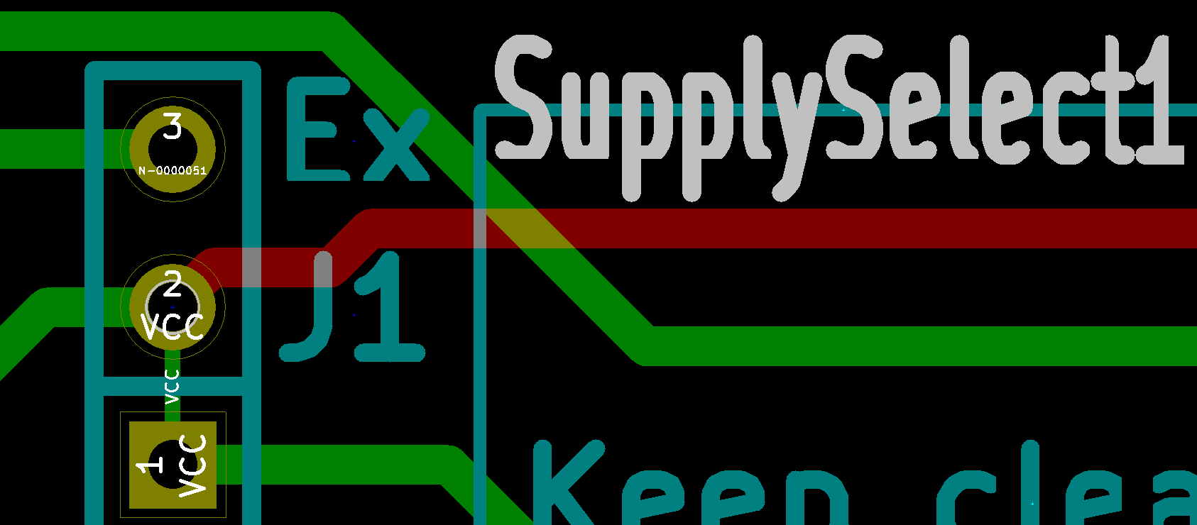
After invoking it, request "File | Load Gerber File", and open, all at once, all of the files you can see in the Plots folder... but you won't, at this stage, see the .drl file, or the .zip file. When you've done that, you should see your board almost as you want it. Now add "on top" of what you have opened so far the .drl file, which is an "Excellon" file, don't worry. Now you should see your board, with the holes... but you could be forgiven for not realizing the holes are shown, if your KiCad has the same color scheme as mine. (See illustration... the holes in the pads are shown... but in nearly the same cyan as the pad itself.)
This is one of your important chances for quality control, and for getting the board you actually wanted, vs the one that was in your KiCad software at the time you made the Gerber files. Be reasonable: How can OSH Park "be nice" about re-doing a board for free, if the only things wrong with it were mistakes on your part in saying what you wanted??
OSH Park's demands are so reasonable, that I can't find much to say about this step, other than to confirm that it is just the "usual" creation of a user account on their system.
Once you have your account, you have a place where you can "store stuff". So, for instance, if later you want more copies of a board you had them make up for you previously, you will find the files there waiting for you.
You start by logging in. And then you click the "Get Started" button. That lets you start a new project... it isn't just for people using OSH Park for the first time.
Remember, as we progress through this step: just uploading your files doesn't place your order. It is a preliminary step.
Your OSH Park account comes with a "page" where you will see a list of the projects you have on their system. Each must be given a name and a description.
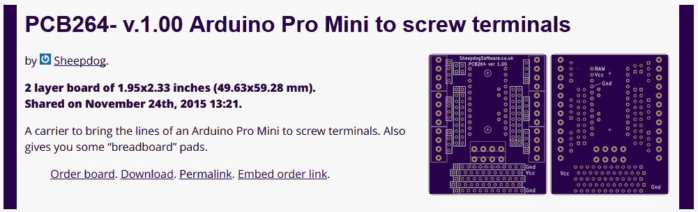
The image to the left is what shows up in my OSH Park account for a project I did earlier. Whatever you enter as Name will appear as the "PCB264... screw terminals" appears in the example. My Description for that project was "A carrier to bring... you some "breadboard" pads."
You can see all of your old projects... and order further copies of the boards. The public can see... and order... and download the Gerbers... for any projects you choose to make public. You (and the public) can search on the text in either. Apparently, 30 Nov 16, I am the only person offering something with the text "carrier to bring"! And the search engine is clever enough to find it, even if you spell bring "brong"! UNLESS you offer the schematic elsewhere, and put a link to that in the description, the public WON'T have direct access to the schematic.
(Edits to the name and description are "live" immediately. The search engine seems to need a little time to become aware of edits, and newly listed projects.)
In some instances, if your files fail to pass the tests we'll come to in a moment, you simply start again, making a "new" project. So if your name or description would be a pain to re-generate, put a copy of them into a text editor for an easy copy/ paste if you have to start again.
You'll get images to show you what it seems your board will probably look like.
This would be a good time to use right-click/ copy image, to capture images of what your board will be like. There are some higher resolution images to come, which you may decide are better for your wants... but because of cropping during the next stage, you may want these to fall back on, as "the best" overall impressions.
The system can't be expected to be foolproof... but, if you are attentive, it will catch many problems for you in the preview. You just go "back to the drawing board", make adjustments to your design, or maybe just to the Gerber and drill file generation, and then re-submit, check the previews again. They are remarkably life-like if all is well. (You "re-submit" by "starting" a "new" project... go to "Home" page, click "Get Started Now" to start a new project. As I said: that "Get Started Now" is not just for people joining the OSH Park customer base for the first time.)
(I continue to write for someone making a two layer board. I haven't done a four layer board, so can't tell you the (probably slight) differences!)
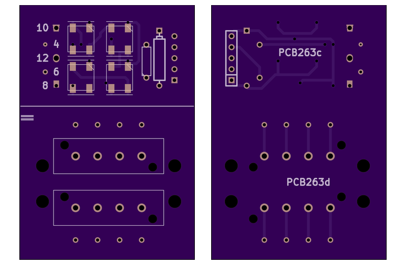
Pay particular attention to the first two images: the one of the top of the board, one of the bottom. I've put the first two from one of my projects on this page. Yes! The boards are purple!
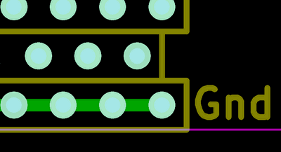
You should see black where there is supposed to be a hole. In my board, there are four small and four large black holes with no copper at their edges. (8 on the board, 16 if you count all such in the illustration showing top and bottom, i.e. each hole twice.) These are mounting holes, and you might not have anything comparable on your board. Look closely, though, and you will see about 30 "normal" holes.
There are traces (tracks) on the board I've used to illustrate this section, but you have to look carefully to see them, as they are under a solder mask. (With KiCad + OSH Park, the masks (top and bottom) "just happen". Don't worry that they are something else to worry about.)
After the first two "overall impression" images, you will get images for each of the layers.
(Don't be alarmed by the fact that in each preview, things will seem to go right to the edge of the board. The previews are cropped, to leave out all "unused" "edge of board" areas. Remember the design spec requirement (at Feb 15) for at least 15 mil clearances from traces to the edge of the board.)
Also easy. You can pay with PayPal or credit card.
It was, for me, on my first attempt. I hope you will have good experiences, too. (And easy again on multiple subsequent uses of the service... latest, as I write this paragraph, November 2016.)
The system is highly automated... so that things run smoothly, and to keep costs down. If you know that you will be doing two (or more) orders within a day or two of each other, if you upload the first, but don't proceed to the "order" phase, you can easily order it when you've uploaded the second and are ready to order that. There's no point in emailing OSH Park to say "feel free to combine in one parcel", as there isn't a way for them (sensibly) to "pick out" the two to do that. But if you order them together, it may happen.
Next time....
I hope your first experience will be good, and that you will go back to do further projects.
Log on. Go to the Home Page. Click the "Get Started" button. This is not just for people new to the site, as you might presume. It is also for starting the process of uploading a subsequent project... and for "revising" a project. (Version 2 of Project A is, within the OSH Park system, treated as a "new" project. You can edit the name and description of an old project, but you can't replace the files associated with it... but you can delete "old" (superceded version) projects from your OSH Park account.)
Make the world a better place! Is your board good for anything? Just by setting up a name to be known by in your "sharing" life, and clicking "Start Sharing" on the board or boards you are willing to release thus, you can allow other people to order "copies" of your board. No hassle for you. (No profit, either, if you "sell" by this route... but you help OSH Park, and they helped you, didn't they!) Apart from putting a small page online with documentation online about what components the board needs, what is it good for, etc. Once you've done that, just put a link to it in the description of the board at your OSH Park "Projects" page. Note what I said above about the Gerber files, but not the schematic, being available to all if you decide to share a project.
![]() Page has been tested for compliance with INDUSTRY (not MS-only) standards, using the free, publicly accessible validator at validator.w3.org. Passes as regards big problems. Some updating to HTML5 standards still needed.
Page has been tested for compliance with INDUSTRY (not MS-only) standards, using the free, publicly accessible validator at validator.w3.org. Passes as regards big problems. Some updating to HTML5 standards still needed.
AND passes...
